Executive summary — what changed and why it matters
Thesis: Apple’s new Fusion Architecture for the M5 Pro and M5 Max deliberately shifts the generational battleground from raw CPU core scaling to paired‑die memory and GPU throughput, recentering the Mac as a device optimized for on‑device AI and graphics. That structural choice changes who controls value and risk: it amplifies developer dependence on platform optimization, concentrates procurement uncertainty around validation windows, and shifts privacy and repair tradeoffs from cloud settings to endpoint governance.
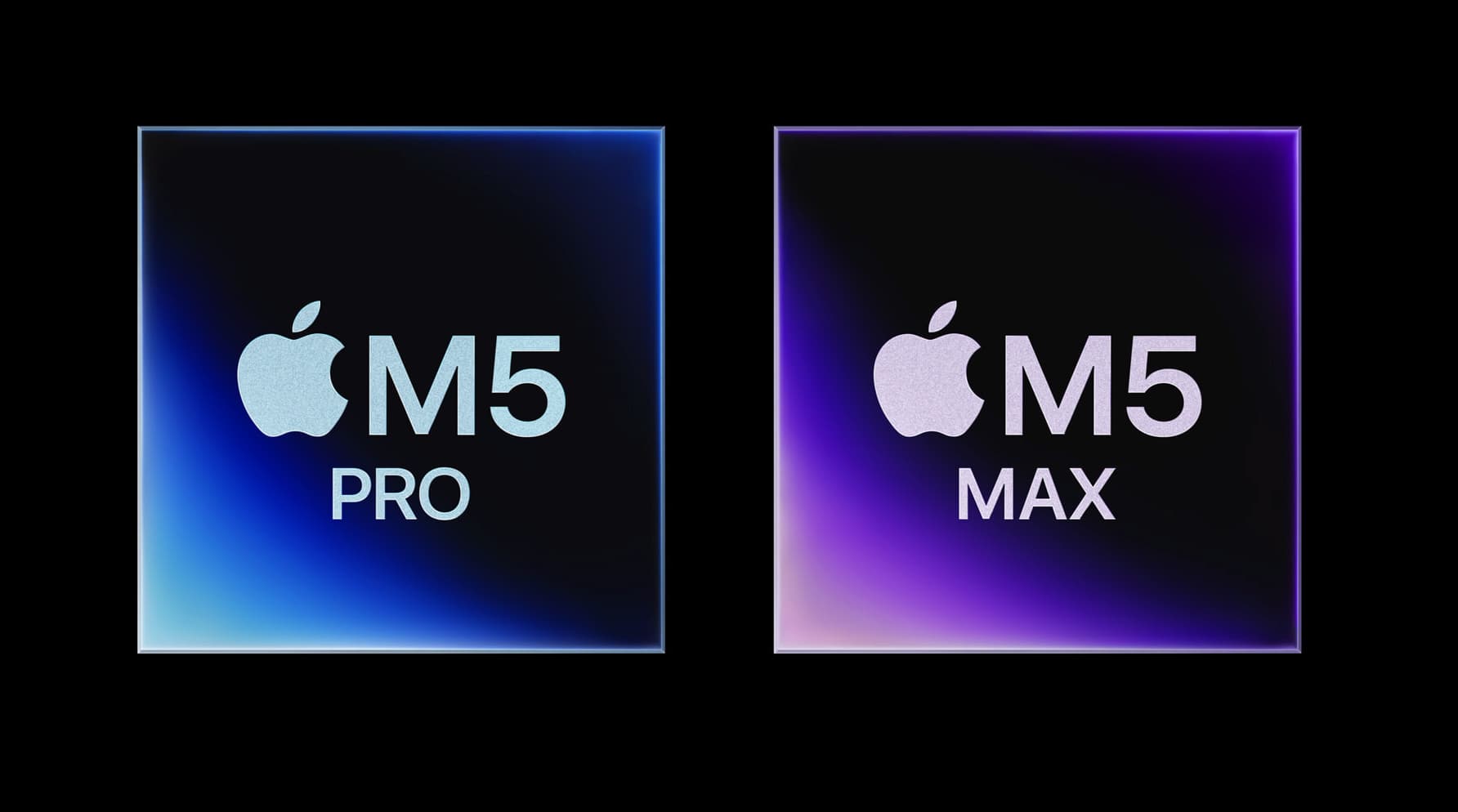
At a hardware level the announcement is specific and narrow: Apple pairs two third‑generation 3nm dies into a single SoC with a high‑bandwidth interconnect, standardizes an 18‑core CPU topology (six “super” plus 12 performance cores), and moves differentiation to GPU and memory. M5 Pro caps out at a 20‑core GPU while M5 Max doubles to 40 GPU cores; memory bandwidth scales from 307GB/s (Pro) to 614GB/s (Max), with the Max supporting up to 128GB of unified memory. Those are the levers Apple used to argue that on‑device AI is now a primary design objective rather than a secondary feature.
What the architecture actually does
Fusion Architecture pairs two dies with a high‑bandwidth, low‑latency interconnect and embeds Neural Accelerator functionality into GPU cores. In practice this means Apple is not pursuing another generation of increasing CPU single‑thread dominance as the headline; instead the company has concentrated investment in wider memory channels and denser GPU arrays that can sustain larger models on a device without offloading to cloud inference.
The practical outputs Apple emphasizes are: higher peak GPU AI compute (Apple-stated “up to 4×” vs M4 Pro), larger unified memory capacity (up to 128GB on M5 Max), and doubled memory bandwidth on the Max (614GB/s). Ray tracing performance is claimed to be up ~35% versus the M4 generation. Apple also says the design integrates Thunderbolt 5 controllers on‑chip and ships with updated wireless silicon (Wi‑Fi 7 and a new N1 wireless chip supporting Bluetooth 6), all framed as supporting heavier on‑device workloads.
Important qualification: the “up to” and peak metrics are Apple’s claims and should be treated as manufacturer‑provided peaks rather than universally representative performance. Independent, sustained benchmarks for single‑core leadership, real‑world LLM inference across representative models, battery life under heavy AI workloads, and long‑term thermal behavior are not yet available in the public domain. Those validation gaps are material because the announcement’s strategy hinges on bandwidth and GPU throughput translating into consistent, deployable gains for users and enterprises.

Key takeaways — diagnostic framing
- Scaling lens: The M5 family shifts the primary scaling vector from CPU microarchitecture gains to multi‑die interconnect, GPU scaling, and memory bandwidth. The difference between Pro and Max is not CPU core count (both use 18 cores) but GPU core count (20 vs 40) and memory bandwidth (307GB/s vs 614GB/s).
- On‑device AI is now a product axis: Embedding Neural Accelerator features into GPU cores and doubling memory bandwidth are explicit engineering choices that privilege inference and model residency on the endpoint over cloud‑centric architectures.
- Performance reality: Apple-cited peaks (e.g., “4× peak GPU AI compute vs M4 Pro”) are vendor‑provided and tied to specific utilization scenarios; early reports of ~3.9–4× LLM inference gains are workload‑dependent and do not substitute for broad, independent benchmarks across model sizes and quantizations.
- Risk concentration: Where gains exist, they concentrate risk in three domains — application optimization (ISV readiness), thermal and battery sustainability, and enterprise manageability (firmware, update/attestation, repairability).
Breaking down the announcement — concrete details and immediate implications
The structural change is straightforward to describe: two 3nm dies joined with a high‑bandwidth interconnect. This permits larger, unified memory pools and wider memory channels without forcing Apple to produce a single monolithic die of commensurate area (and yield) cost. The M5 Max’s 614GB/s memory bandwidth and 128GB unified memory address workloads that need model weights and working memory resident on the device—large video or machine‑learning models that otherwise would be shuttled across slower I/O to local or cloud accelerators.
GPU scaling becomes the primary performance differentiator: 20 GPU cores in the Pro and 40 in the Max. That delta is how Apple claims the Max achieves much higher peak GPU AI throughput. At the same time, CPU generational gains are modest in comparative terms: the company’s own materials indicate the M5 Max’s multithreaded CPU performance is roughly +15% versus the M4 Max, while the advertised GPU/AI uplifts are much larger on paper.
Apple additionally highlights a 35% ray tracing improvement over the previous generation. That specific graphics claim is one of the more concrete ratios provided in the launch coverage; it signals Apple intends these chips to be meaningful for creative workflows that depend on ray‑traced previews, not just AI inference.
Competitive angle and market context — diagnostics with metrics
Compared with prior Apple silicon (M4 line), the M5 family intentionally reframes the competitive argument toward throughput rather than headline CPU IPC or single‑thread metrics. The architecture is designed so that a device with an 18‑core CPU and a 40‑core GPU coupled to 614GB/s of memory bandwidth can host larger models and sustain higher GPU utilization without external hardware.
Against x86 + discrete GPU workstations, the tradeoffs are clearer when grounded in the numbers Apple supplied. Apple’s value proposition rests on unified memory and the latency benefits of integrated interconnect—40 GPU cores coupled to 614GB/s of unified memory creates a simpler data path for models than a CPU + discrete GPU with separate VRAM. That simplifies some developer assumptions (no explicit copy between CPU and GPU memory) and changes software engineering tradeoffs.
Diagnostics: discrete GPUs still dominate certain raw‑throughput and price‑sensitivity niches—workstations optimized for maximum rasterization or massively parallel raster/compute can still be less expensive on a price‑per‑raw‑GFLOP basis. Apple’s announcement does not provide broad head‑to‑head pricing or exhaustive throughput comparisons versus specific discrete GPUs; the practical comparison should include measured sustained throughput, driver maturity for professional ISVs, and total system cost of ownership rather than peak vendor figures alone.
Human stakes — who gains and who risks losing control
The moves embedded in Fusion Architecture change the locus of agency across the ecosystem:
- Developer agency: ISVs and toolmakers now face a stronger incentive to optimize their stacks for Apple’s unified memory and GPU/accelerator topology. That optimization often implies additional engineering effort and tests targeted at macOS‑specific synchronizations, memory management, and quantization regimes. The result is a potential split in developer attention: further investment in macOS optimizations could deepen Apple lock‑in for creative and ML tooling.
- Enterprise agency: On‑device AI reduces cloud round trips and gives organizations the capability to process sensitive data locally, which can increase control over privacy. But that control is conditional on firmware update policies, secure‑boot and attestation behavior, and repairability. If enterprises lack transparency or influence over those device governance elements, shifting workloads to endpoints simply changes where control is exercised, not necessarily who holds it.
- Operational identity and skills: IT and MDM teams may need to reconcile on‑device inference capabilities with existing compliance and dataflow policies, shifting some responsibilities from cloud architects to endpoint managers. Repair and sustainment professionals may face higher complexity because the Fusion dual‑die approach can change diagnostic, repair, and replacement profiles compared with single‑die SoCs or modular components.
Risks, governance and operational considerations
Several risk vectors emerge from the Fusion Architecture strategy and from gaps in independent validation:
- Validation gap: Key claims—single‑core leadership, battery life under sustained AI loads, and the real‑world consistency of “up to” GPU AI multipliers—are vendor‑reported and lack broad, independent verification. These gaps matter for procurement confidence because the headline metrics are highly dependent on workload mix, model size, and power/thermal envelopes.
- Thermal and sustainment tradeoffs: Dual‑die designs can change thermal distribution, potentially creating new hotspots or shifting throttling behavior. Sustained high GPU utilization for large model inference is where battery and thermals will most likely reveal differences between peak and sustained performance.
- ISV and ecosystem readiness: Productivity gains from on‑device LLMs require ISV optimizations, model quantization strategies, and compatibility testing. Absent broad ISV certification, enterprises may face a period where nominal device capability does not translate into measurable productivity improvements.
- Repairability and service cost: The pairing of dies and tighter integration with on‑chip controllers (Thunderbolt 5, wireless) could increase service complexity and costs, with consequences for uptime, technician workflows, and secondary‑market resale value.
Recommendations — diagnostic framing and common organizational responses
The following section frames common organizational behaviors and decision heuristics that typically follow an architecture shift of this kind. These are descriptive and evidence‑aligned statements about how buyers and operators commonly react given the validation gaps and risk vectors identified above.
- Procurement conservatism is typical: Organizations purchasing large fleets often adopt a validation window (commonly measured in weeks to months) after a new silicon launch to gather independent benchmarks, ISV certifications, and thermal/battery reports before commits. This behavior mitigates the risk that vendor peak claims do not map to sustained, deployable performance.
- Targeted pilots emerge as the de‑risking pattern for specialist workloads: Creative teams and ML groups frequently pilot higher‑spec models (e.g., configurations with 128GB unified memory and the Max GPU) on representative projects to validate compatibility and effective throughput before broader rollouts. That pilot‑first approach is a diagnostic step rather than a prescriptive rule.
- Security and manageability reviews become more detailed: IT/security teams commonly request vendor documentation on firmware update cadence, secure boot and attestation mechanisms, and repair workflows when a device increases on‑device processing of sensitive data. Those requests reflect a shift in endpoints’ role in data governance, not simply a change in performance profile.
- Expectation calibration for ISVs: Organizations relying on ISV productivity gains typically expect a lag between silicon availability and optimized application releases. Planning for this developer lead time is a normal governance step when platform shifts increase API and memory‑model dependencies.
What to watch next — resolving the uncertainty
The critical events that will either validate or limit Fusion Architecture’s practical impact are concrete and measurable:
- Independent benchmarks for LLM inference across a representative set of models and quantization strategies, including measurements of sustained latency, throughput, and power consumption.
- ISV announcements and certifications from major creative and professional applications—Adobe, Autodesk, DaVinci, and entrant ML toolmakers—that explicitly document optimization and validated workflows on M5 hardware.
- Sustained thermal and battery tests that show how peak GPU utilization maps to real‑world session times and throttling behavior under creative and AI workloads.
- Vendor transparency about firmware update processes, attestation APIs, and repairability documentation that affect enterprise governance and lifecycle management.
Conclusion — a reorientation, not an inevitability
Apple’s Fusion Architecture represents a conscious reorientation of the Mac’s hardware priorities: the company is turning a generational cadence into a platform bet that wider memory bandwidth and denser GPU arrays, made possible by paired dies, will unlock on‑device AI as a differentiator. That move has meaningful human stakes—shifting developer effort, altering enterprise control over data and device governance, and concentrating procurement risk around validation windows.
Whether Fusion becomes a decisive shift in how organizations work will depend less on Apple’s peak figures and more on the slower, human parts of the ecosystem: ISV optimization timelines, sustained thermal and battery performance in real‑world workflows, and the degree to which enterprises can exercise governance over firmware and repairability. Those are the points that will determine whether Fusion is a practical accelerant for on‑device AI or primarily a marketing‑driven framing of incremental hardware improvements.